Complete Dual-Band
Quadrature Transmitter
______________________________________________________________________________________ 15
t
CS
t
CH
t
CWL
t
CWH
DI
NOTE: THE 3-WIRE BUS IS SPI/QSPI/MICROWIRE-COMPATIBLE.
CLK
CS
t
ES
B19 (MSB)
B18
B0
A3
A1
A0 (LSB)
t
CS
> 50ns
t
CH
> 10ns
t
CWH
> 50ns
t
ES
> 50ns
t
CWL
> 50ns
t
EW
> 50ns
t
EW
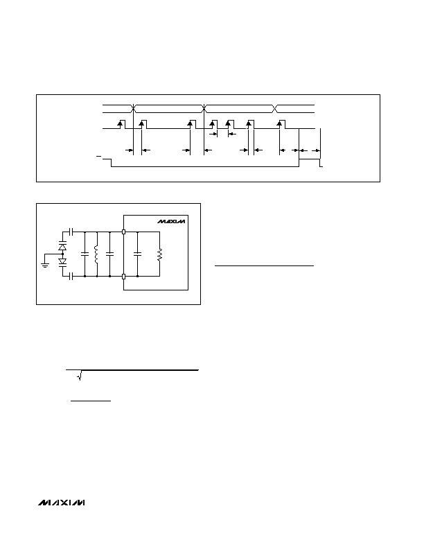
Figure 3. 3-Wire Interface Diagram
IF Tank Design
The IF VCO tank (TANK+, TANK-) is fully differential.
The external tank components are shown in Figure 4.
The frequency of oscillation is determined by the follow-
ing equation:
C
INT
= Internal capacitance of TANK port
C
D
= Capacitance of varactor
C
VAR
= Equivalent variable tuning capacitance
C
PAR
= Parasitic capacitance due to PC board pads
and traces
C
CENT
= External capacitor for centering oscillation fre-
quency
C
C
= External coupling capacitor to the varactor
Internal to the IC, the charge pump will have a leakage
of less than 10nA. This is equivalent to a 300M& shunt
resistor. The charge-pump output must see an
extremely high DC resistance of greater than 300M&.
This will minimize charge-pump spurs at the compari-
son frequency. Make sure there is no solder flux under
the varactor or loop filter.
Layout Issues
The MAX2369 EV kit can be used as a starting point for
layout. For best performance, take into consideration
power-supply issues, as well as the RF, LO, and IF lay-
out.
Power-Supply Layout
To minimize coupling between different sections of the
IC, the ideal power-supply layout is a star configuration,
which has a large decoupling capacitor at a central
V
CC
node. The V
CC
traces branch out from this node,
each going to a separate V
CC
node in the MAX2369
circuit. At the end of each trace is a bypass capacitor
with impedance to ground less than 1& at the frequen-
cy of interest. This arrangement provides local decou-
pling at each V
CC
pin. Use at least one via per bypass
capacitor for a low-inductance ground connection.
Matching Network Layout
The layout of a matching network can be very sensitive
to parasitic circuit elements. To minimize parasitic
inductance, keep all traces short and place compo-
nents as close to the IC as possible. To minimize para-
sitic capacitance, a cutout in the ground plane (and
any other planes) below the matching network compo-
nents can be used.
On the high-impedance ports (e.g., IF inputs and out-
puts), keep traces short to minimize shunt capacitance.
f
2 (C
C
C
C ) L
C
C
C
2 (C + C )
OSC
INT
CENT
VAR
PAR
VAR
D
C
D
C
=
+
+
+
=
?/DIV>
1
?/DIV>
L
C
D
C
CENT
C
PAR
C
C
C
C
C
D
MAX2369
C
INT
-R
n
Figure 4. Tank Port Oscillator
发布紧急采购,3分钟左右您将得到回复。
相关PDF资料
MAX2850ITK+
TRANSMITTER MIMO 5GHZ 4CH 68TQFN
MAX7057ASE+T
IC TRANSMITTER ASK/FSK 16-SOIC
MBA-2060
ANTENNA METROLOGY BICONICAL
MC33493ADTBER2
IC RF TRANSMITTER UHF 14-TSSOP
MDEV-916-ES
KIT MASTER DEVELOP 916MHZ ES SRS
MICRF102YM TR
IC TRANSMITTER ASK UHF 8-SOIC
MICRF112YMM TR
IC XMITTER UHF ASK/FSK 10-MSOP
MICRF405YML TR
TRANSMITTER ASK/FSK 24-MLF
相关代理商/技术参数
MAX2369EGM-D
功能描述:射频发射器 RoHS:否 制造商:Micrel 类型:ASK Transmitter 封装 / 箱体:SOT-23-6 工作频率:300 MHz to 450 MHz 封装:Reel
MAX2369EGM-TD
功能描述:射频发射器
RoHS:否 制造商:Micrel 类型:ASK Transmitter 封装 / 箱体:SOT-23-6 工作频率:300 MHz to 450 MHz 封装:Reel
MAX2369EGM-TDG069
制造商:Rochester Electronics LLC 功能描述: 制造商:Maxim Integrated Products 功能描述:
MAX236C/D
功能描述:RS-232接口集成电路 +5V Pwrd 4 RS-232 Xmttrs and 3 RS-232 Rcvrs w/ Pwr Shtdwn & Rcvr RoHS:否 制造商:Exar 数据速率:52 Mbps 工作电源电压:5 V 电源电流:300 mA 工作温度范围:- 40 C to + 85 C 安装风格:SMD/SMT 封装 / 箱体:LQFP-100 封装:
MAX236C/D DIE
制造商:Maxim Integrated Products 功能描述:
MAX236C/D+
功能描述:RS-232接口集成电路 RoHS:否 制造商:Exar 数据速率:52 Mbps 工作电源电压:5 V 电源电流:300 mA 工作温度范围:- 40 C to + 85 C 安装风格:SMD/SMT 封装 / 箱体:LQFP-100 封装:
MAX236CNG
功能描述:RS-232接口集成电路 RoHS:否 制造商:Exar 数据速率:52 Mbps 工作电源电压:5 V 电源电流:300 mA 工作温度范围:- 40 C to + 85 C 安装风格:SMD/SMT 封装 / 箱体:LQFP-100 封装:
MAX236CNG+
功能描述:RS-232接口集成电路 5V MultiCh RS-232 Driver/Receiver RoHS:否 制造商:Exar 数据速率:52 Mbps 工作电源电压:5 V 电源电流:300 mA 工作温度范围:- 40 C to + 85 C 安装风格:SMD/SMT 封装 / 箱体:LQFP-100 封装: